
 Sign In

 Shop
Shop

 Academy
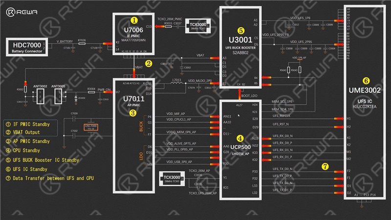
T110 Boot Circuit Working Process
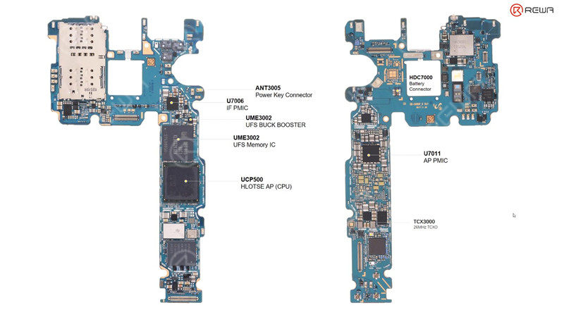
Firstly, let's take a look at UFS or the boot circuit related components on the motherboard. The first one is the battery connector because it's the connection between the battery and motherboard and the direct power source is from the battery. So this one is very important and the second one is IF PMIC which is mainly responsible to provide the VBAT power for the AP PMIC USF Buck boost IC and provide the VBAT power to the power on related contacts. Then is power key contact and actually here, this contact and this contact. They are all related with the power on process.
For details we will introduce in the boot process. This one is AP PMIC. It's mainly used to provide power for the CPU. Then the CPU, UCP500. It's mainly controls the whole boot process and to communicate with the UFS to extract some boot program or the operation system information, etc.
The UFS Memory IC is mainly used to store the boot program and operation system, etc. And this tiny chip, it's called UFS Buck Boost IC. It's mainly used to provide power for the UFS memory IC. And besides that, we also have a crystal TCX3000. It will be used to provide the frequency for the CPU and IF PMIC. So these are the main components that are related to the boot process.
Then let's continue to come to the block diagram to see the detailed working process. And the working process can be divided into different stages.
The first stage is IF PMIC should be standby to work and standby conditions for the chip included with power and frequency provided by this crystal.
First is power, it's provided by the battery. As we can see, the power name is V_BATTERY. And after getting through this resistor it will be seen to the IF PMIC
and this crystalwill provide the working frequency for this IF PMIC.
So with two conditions fulfilled this one will be standby to work. And the second step it will be start to output the VBAT to different chips. As we can see, the VBAT is mainly separated into three branches. One is sent to the buck-boost IC another one is sent to the AP PMIC. Also, as we mentioned, the third branch it will be sent to this contact. This is mainly related with power on trigger signal. These two conditions - the V_BATTERY and VBAT. These two voltage we can measure the voltage values even before pressing down the power button.
Then let's come to see the third stage. The third stage is AP PMIC should be standby to work. And working conditions for this chip is just similar as this one. First, it should get power supplied. And as we can see the VBAT has been sent to the chip directly. And then second one is power on single. So for this power on signal, let's have an introduction about the details and here these two contacts. Before we pressing down the power key button the voltage on this contact is 0 volt. And after we pressing down the power key button these two connects will be connected. So the voltage will be pull up to the VBAT.
After holding it for a few seconds then release the voltage here will be dropped to 0 volt. So the process of pressing the power key button with the voltage change something like this. So the pressing power key button process is to generate the PWR_ON single. And, besides that the crystal should also provide a working frequency for the AP PMIC. So with power, PWR_ON and the frequency fulfilled. AP PMIC will be standby to work then the 4th stage the CPU should be standby to work.
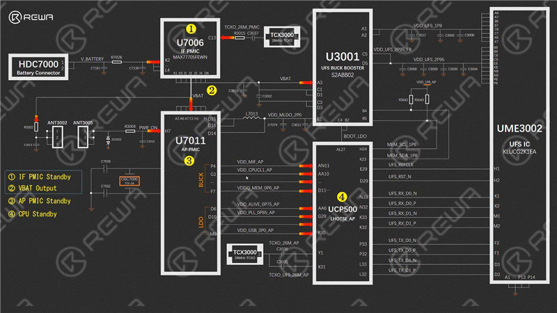
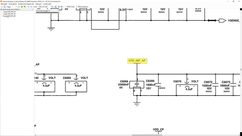
And working conditions is also the same. The powers always come to the first. And as we can see, there are BUCK powers and LDO powers will be outputted from the AP PMIC to the CPU. And here, as we can see some power rails that get vanished because space here is limited. So if you want check the rest power rails and the related components on the power rails, you can go to the schematic to check the details. For example, let's search the VDD_MIF_AP. So you can see it's outputted from the AP PMIC, U7011. And it will be outputted to the CPU. Here's the pins of the CPU. And we can see also there are some details some related components connected with this rail. And with power supply fulfilled then this crystal will also provide the frequency for the CPU.
So, with power and related frequency fulfilled CPU will be standby to work. Then 5th stage is UFS buck boost IC should be standby to work. And working conditions for the UFS buck boost IC is also similar. As we mentioned at the beginning one power is VABT. Another power is VDD_MLDO_2P0. So this is the two powers for the buck boost IC also a BOOT_LDO signal will be outputted from the CPU to the buck boost IC. Besides that, the UFS buck boost IC should be also controlled by CPU through the I2C Bus. And here, as we can see this is a typical structure for the I2C bus with some pull-up resistors on the relative rails. And with SCL and SDA, so now with the power, BOOT_LDO signal and I2C control signal fulfilled. then the UFS buck boost IC will be standby to work. Then the 6th stage UFS IC should be standby to work. So first is power. As we can see, the buck boost IC will provide two powers for the UFS IC. After power, A reference clock signal will be outputted from CPU also a reset signal. So for now, the UFS IC will be standby to work.
Then the last stage is the data transmission between the UFS and CPU just like mentioned before some boot programs or the operation system information will be transmitted between the CPU and the UFS IC. As we can see the signal direction is also different. Here is for the reception or receive and here is for a transmission. This is the working process for the boot circuit and the working process of this circuit.
Please visit REWA Academy for more Android course content.


No Comments
3
1
Share
Apr 23, 2021
ABOUT REWA
REWA is a world leading electronics repair business solutions provider who was founded in 2008 in HongKong. We are committed to delivering one-stop services covering Sourcing Solution, Technical Support Solution as well as Recycle & Resell Solution.


